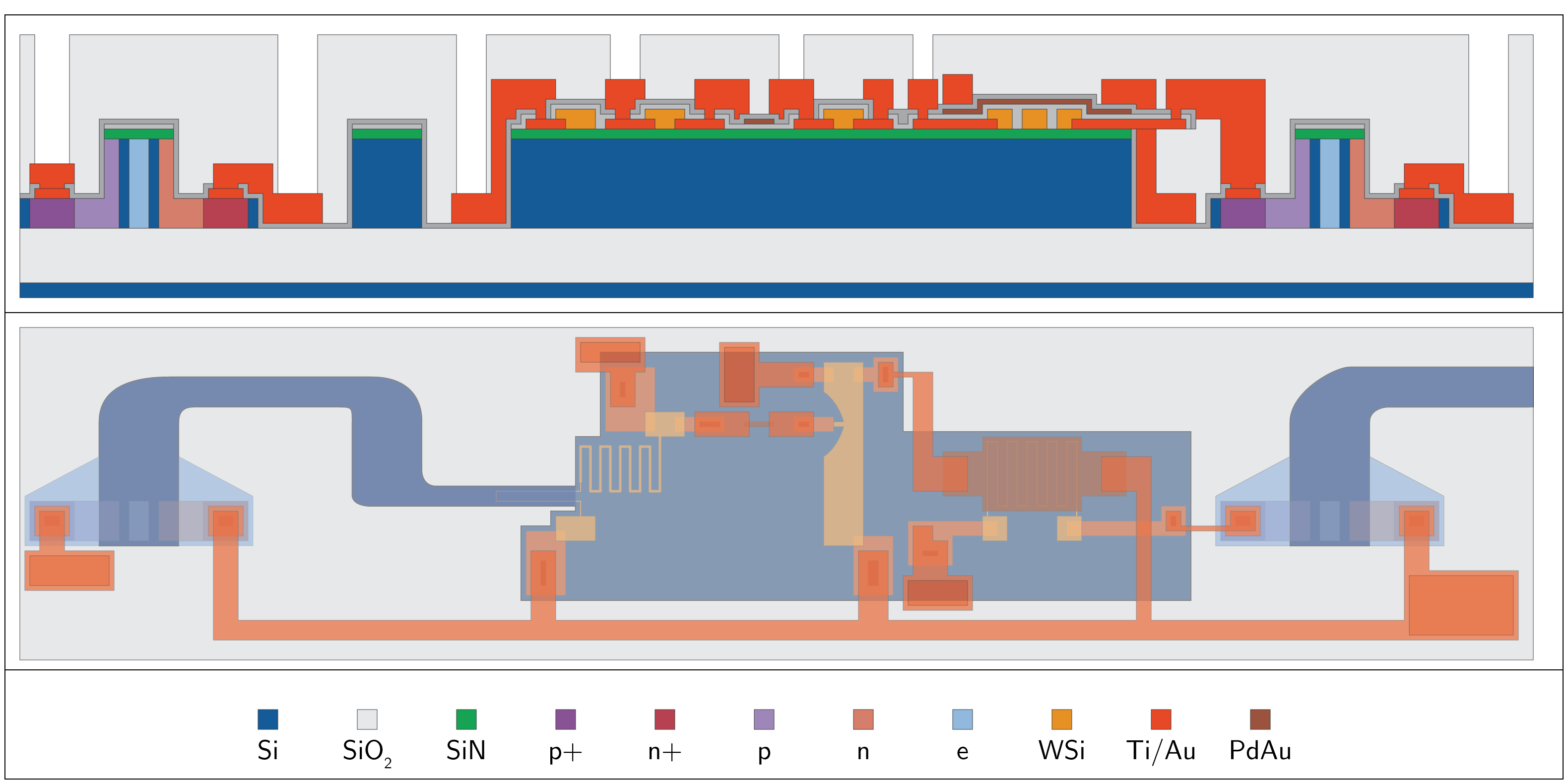
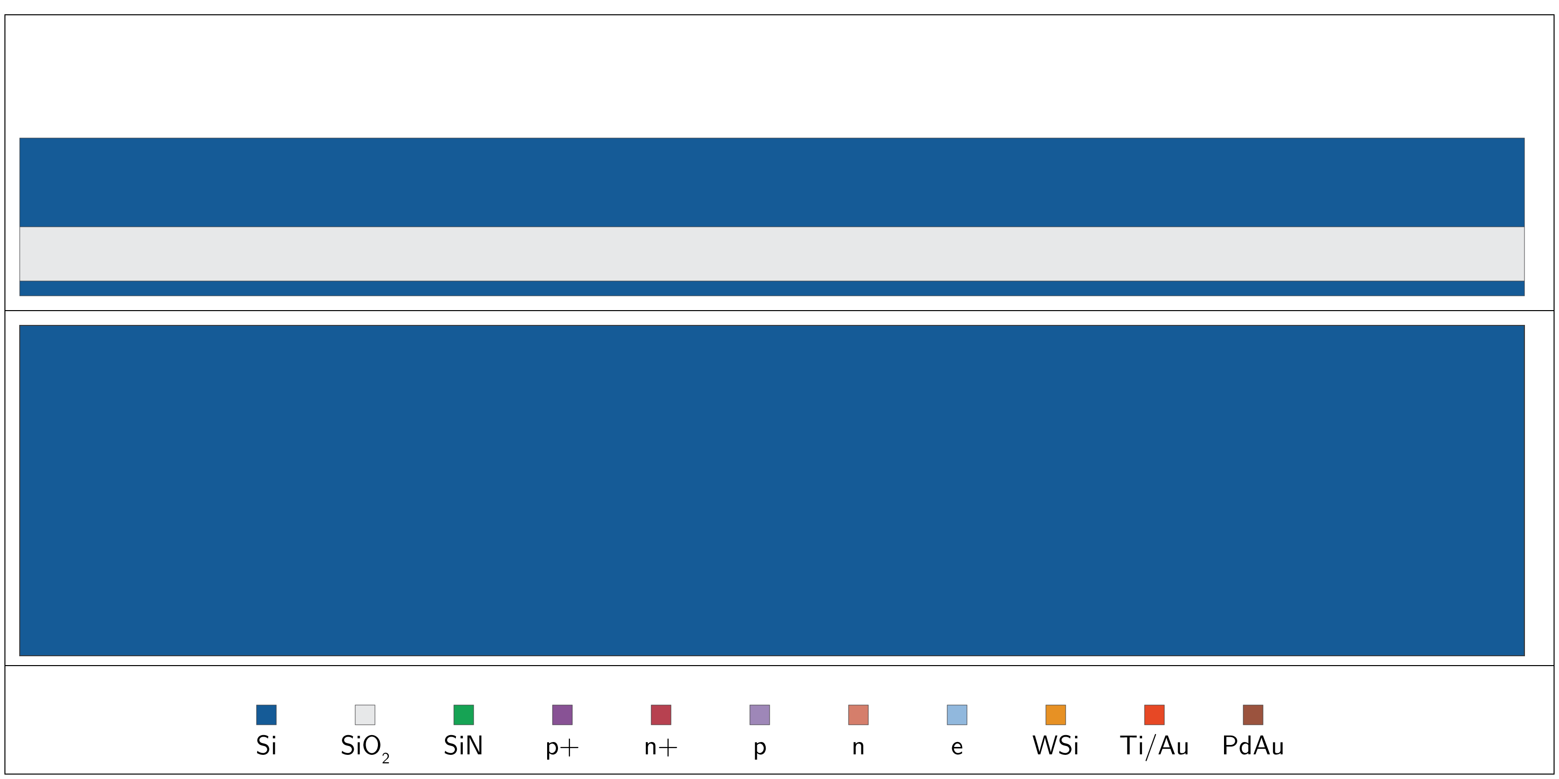
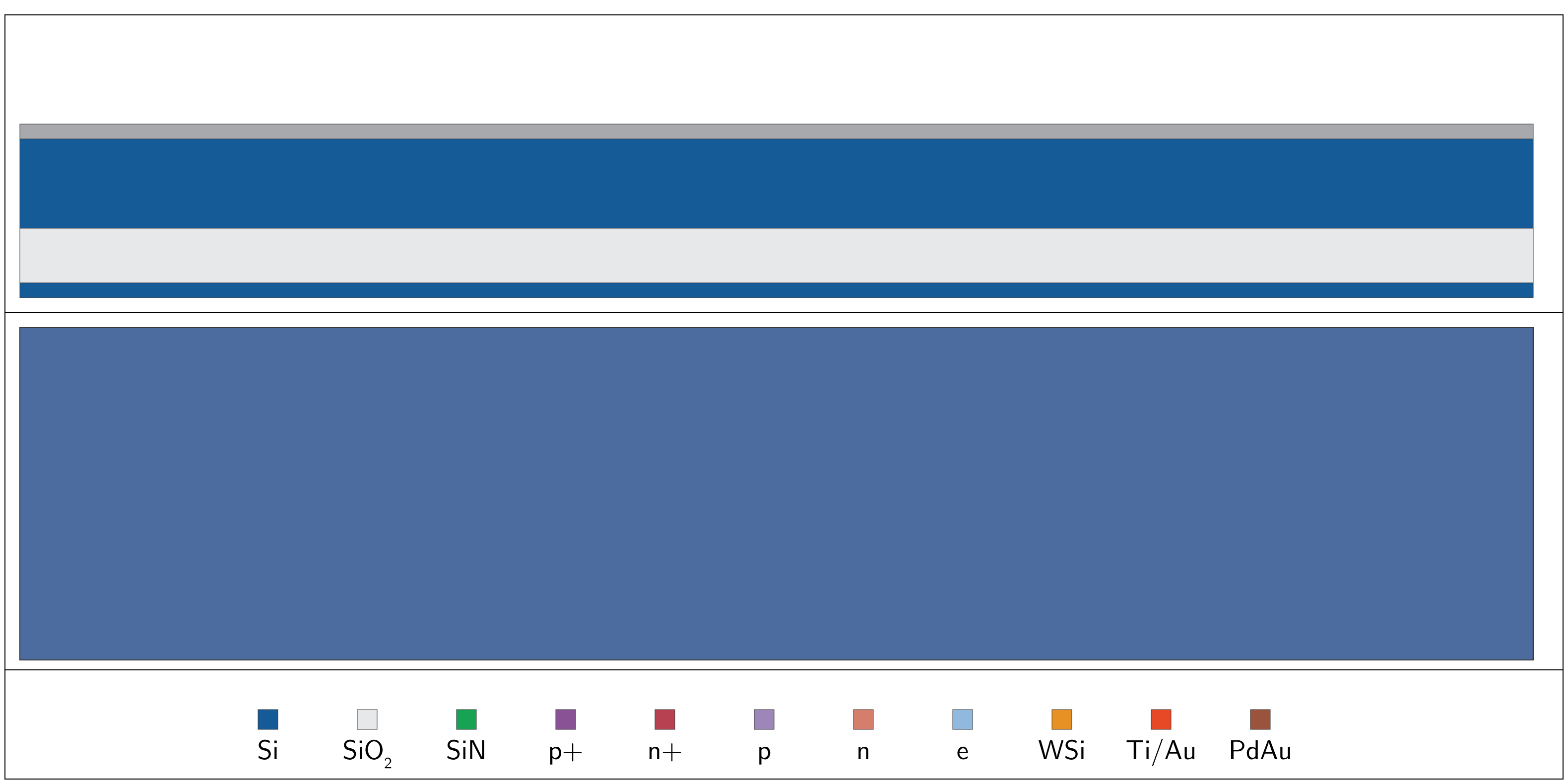
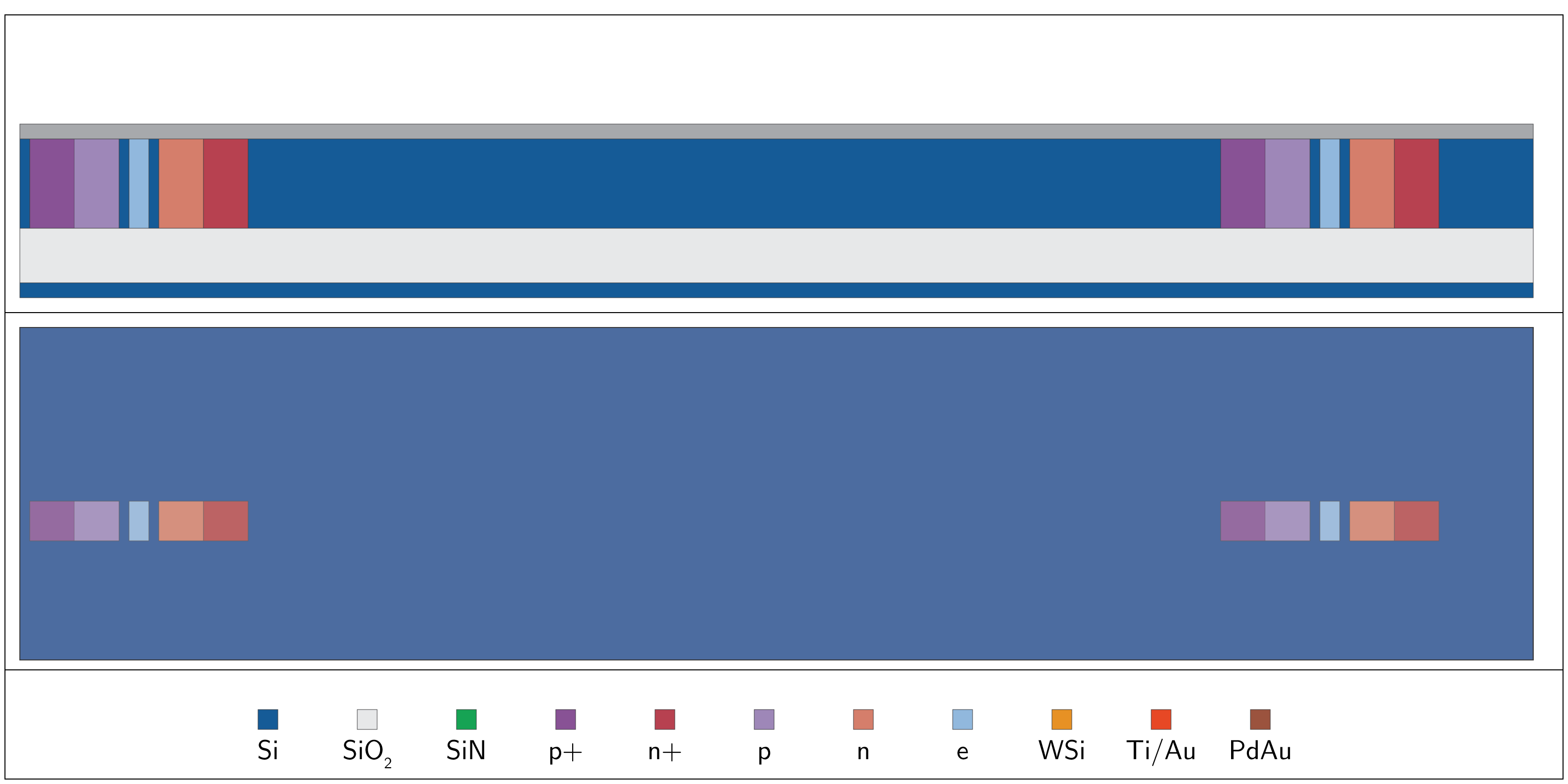
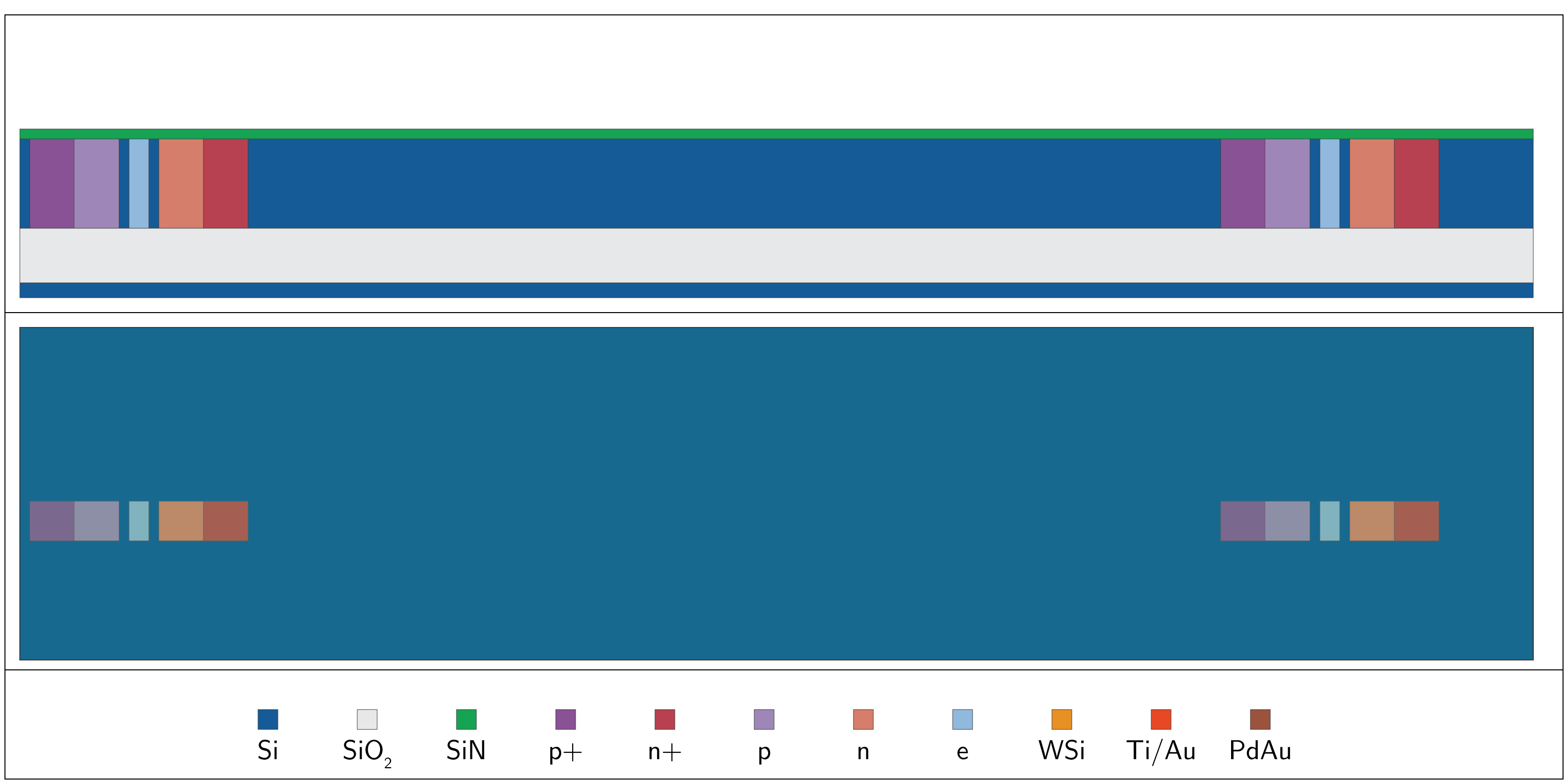
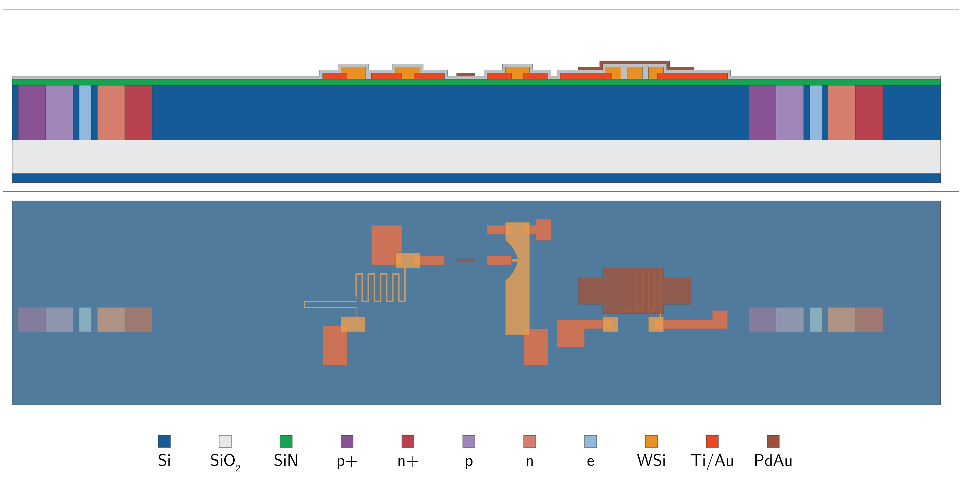
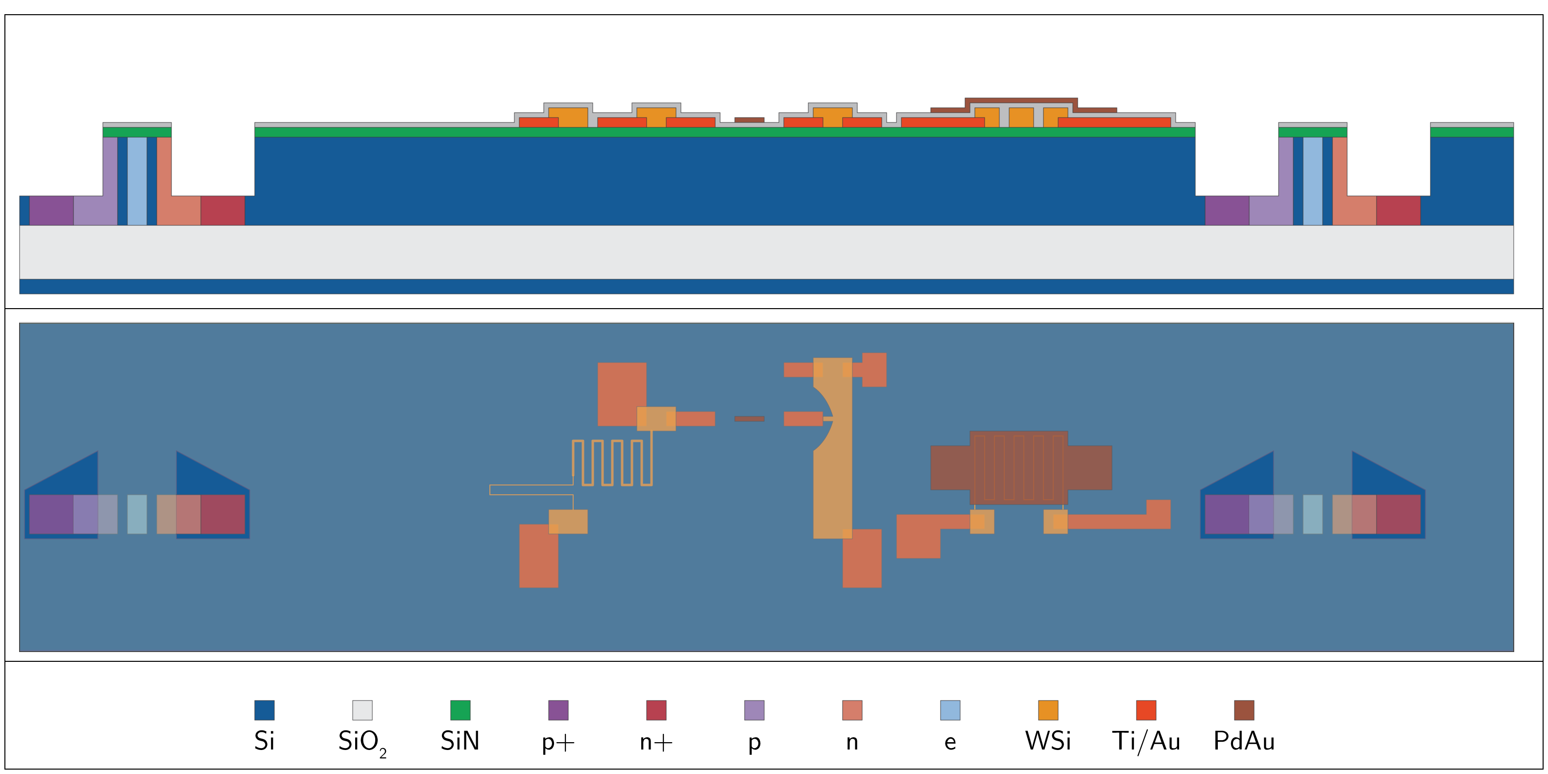
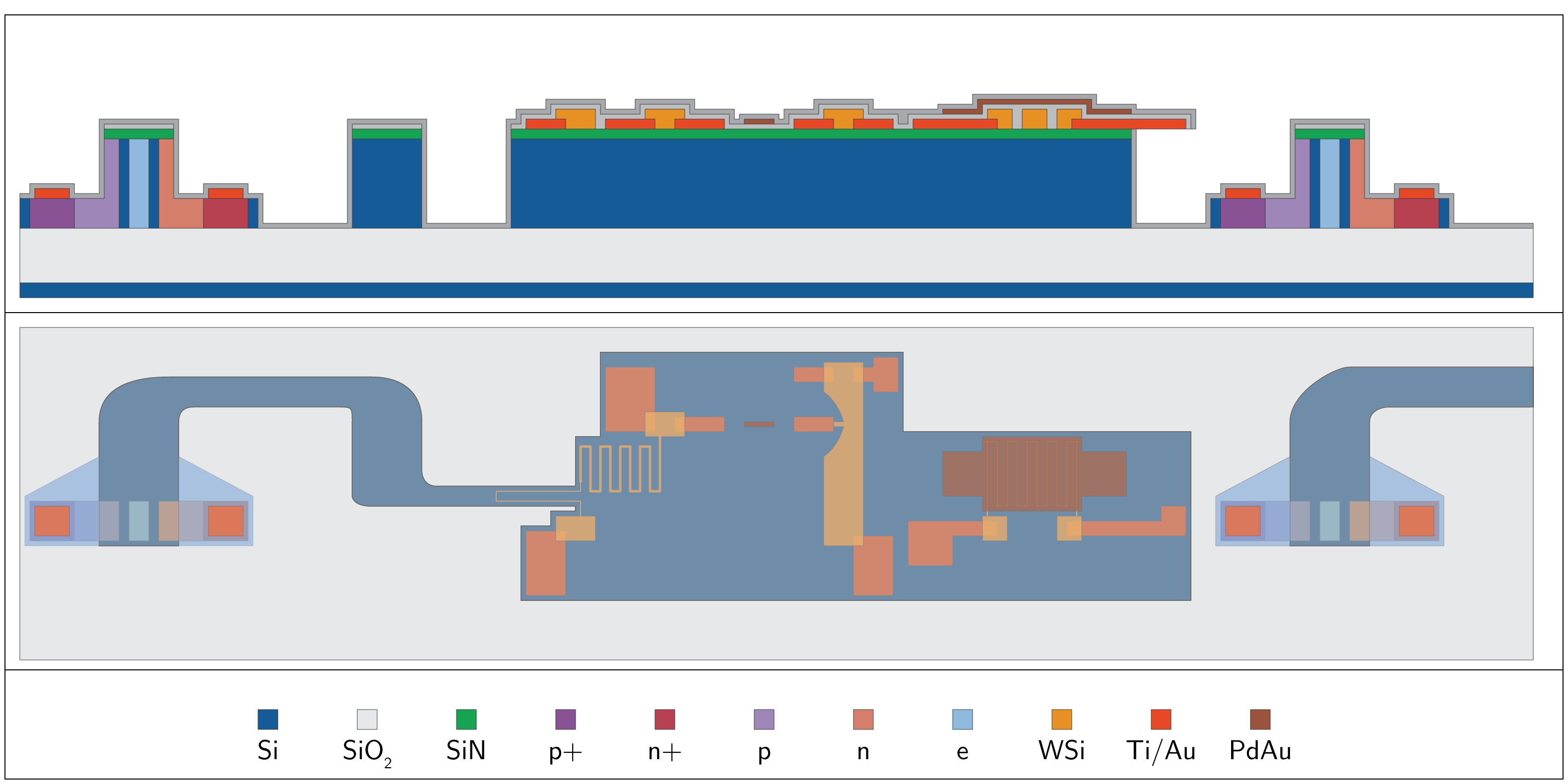
Fabrication steps

These images illustrate each step. The top panels are side view and bottom are top view.

Start with SOI wafer

../../_images/olmc_flowImages_01-si.png

Deposit protective oxide

../../_images/olmc_flowImages_02-protectiveSiO2.png

Implant dopants for P-Si, N-Si, and W-centers. Anneal

../../_images/olmc_flowImages_03-dopants.png

Strip protective oxide and dep SiN etch stop

../../_images/olmc_flowImages_04-barrierSiN.png

Liftoff TiAu small pads for superconductor contacts

../../_images/olmc_flowImages_05-WSiContact.png

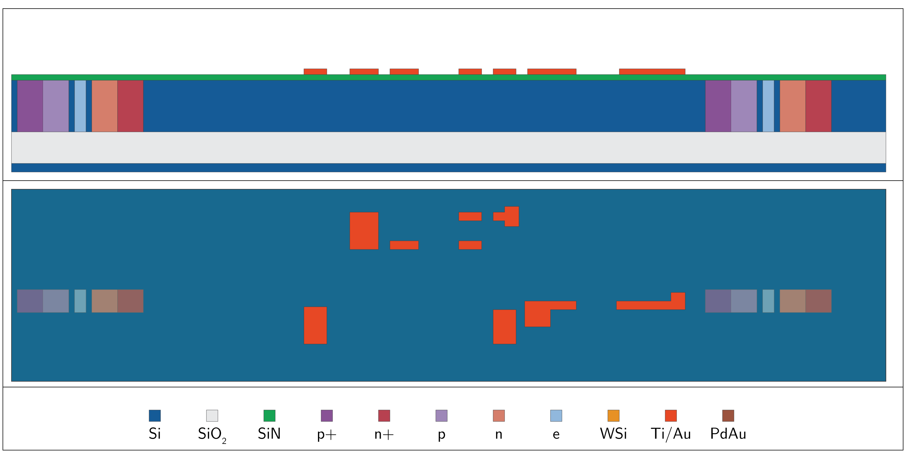
Deposit and pattern WSi superconductor

../../_images/olmc_flowImages_06-WSi.png

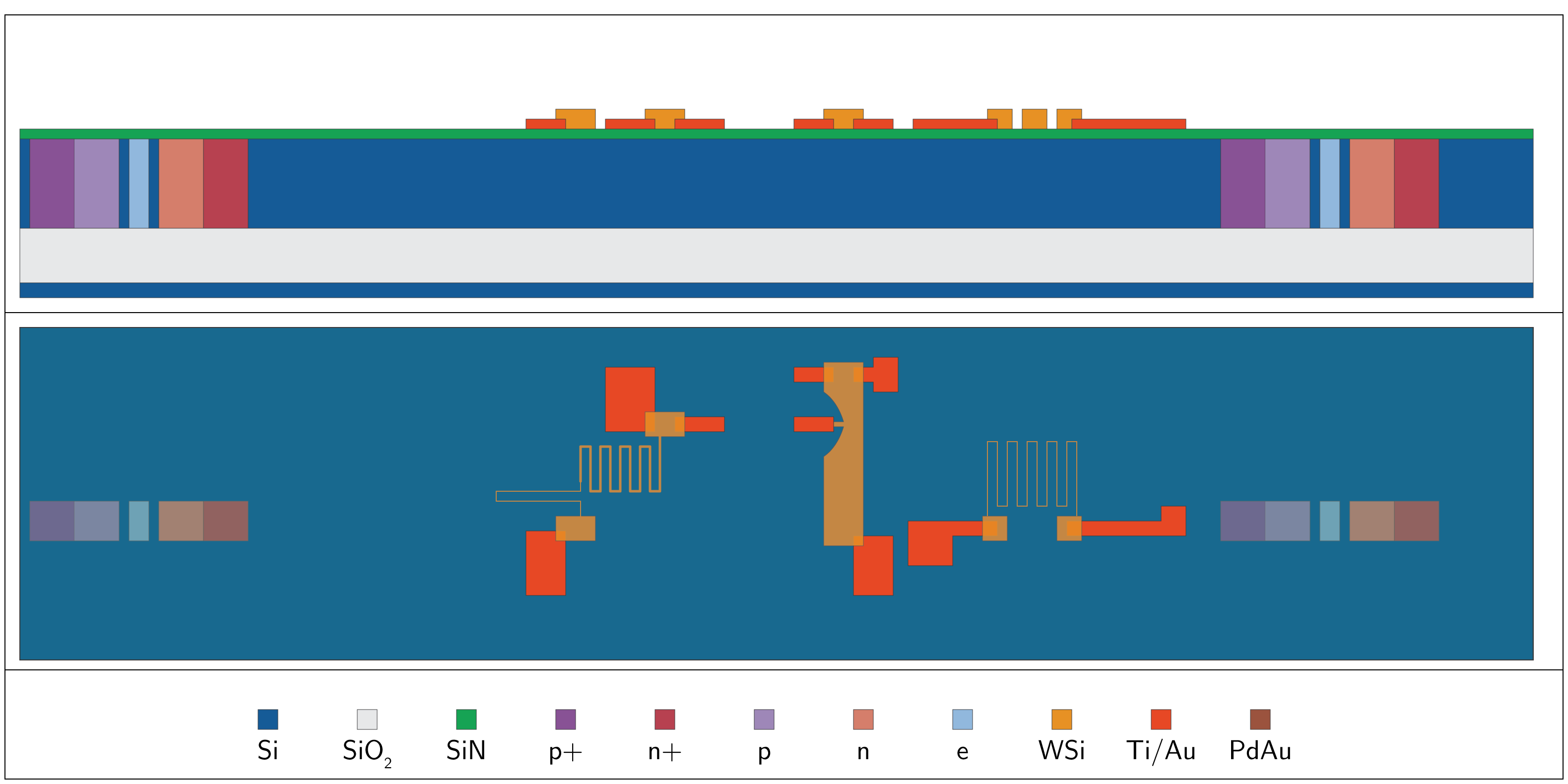
Deposit hTron spacer oxide

../../_images/olmc_flowImages_07-hTronOxideSpacer.png

Lifto􏰀ff resistor layer

../../_images/olmc_flowImages_08-resistor.png

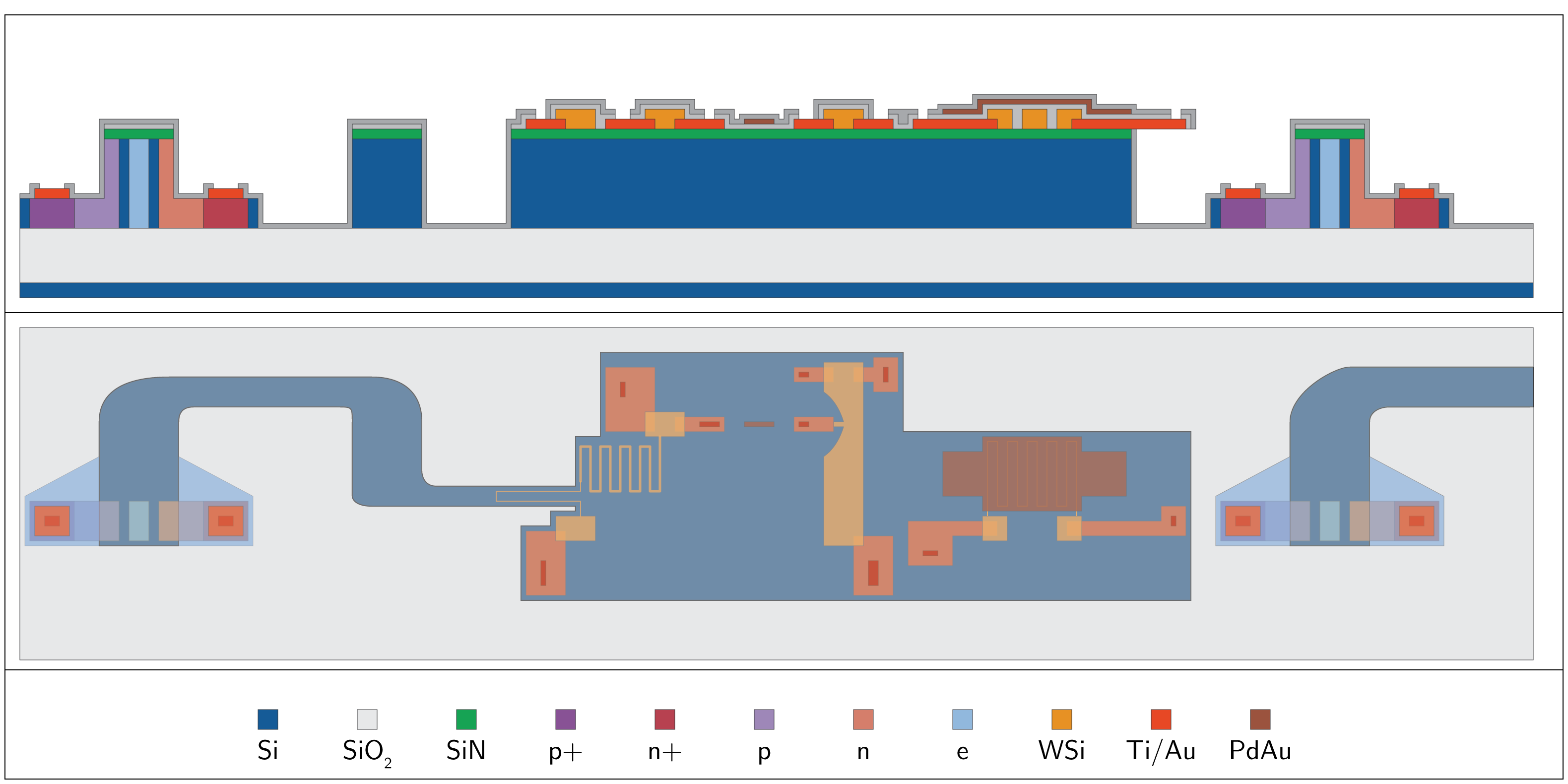
Partial etch for LEDs and waveguides

../../_images/olmc_flowImages_09-partialEtch.png

Full etch for waveguides

../../_images/olmc_flowImages_10-fullEtch.png

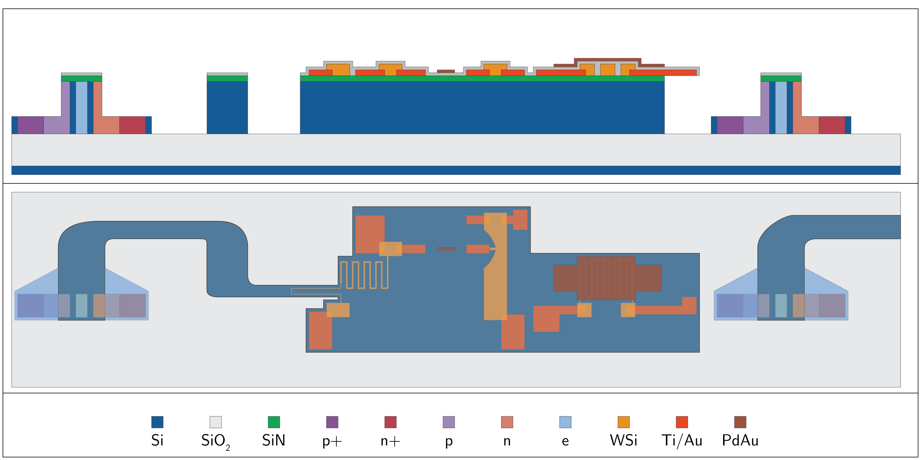
Deposit TiAu small pad for LED contacts

../../_images/olmc_flowImages_11-LEDContact.png

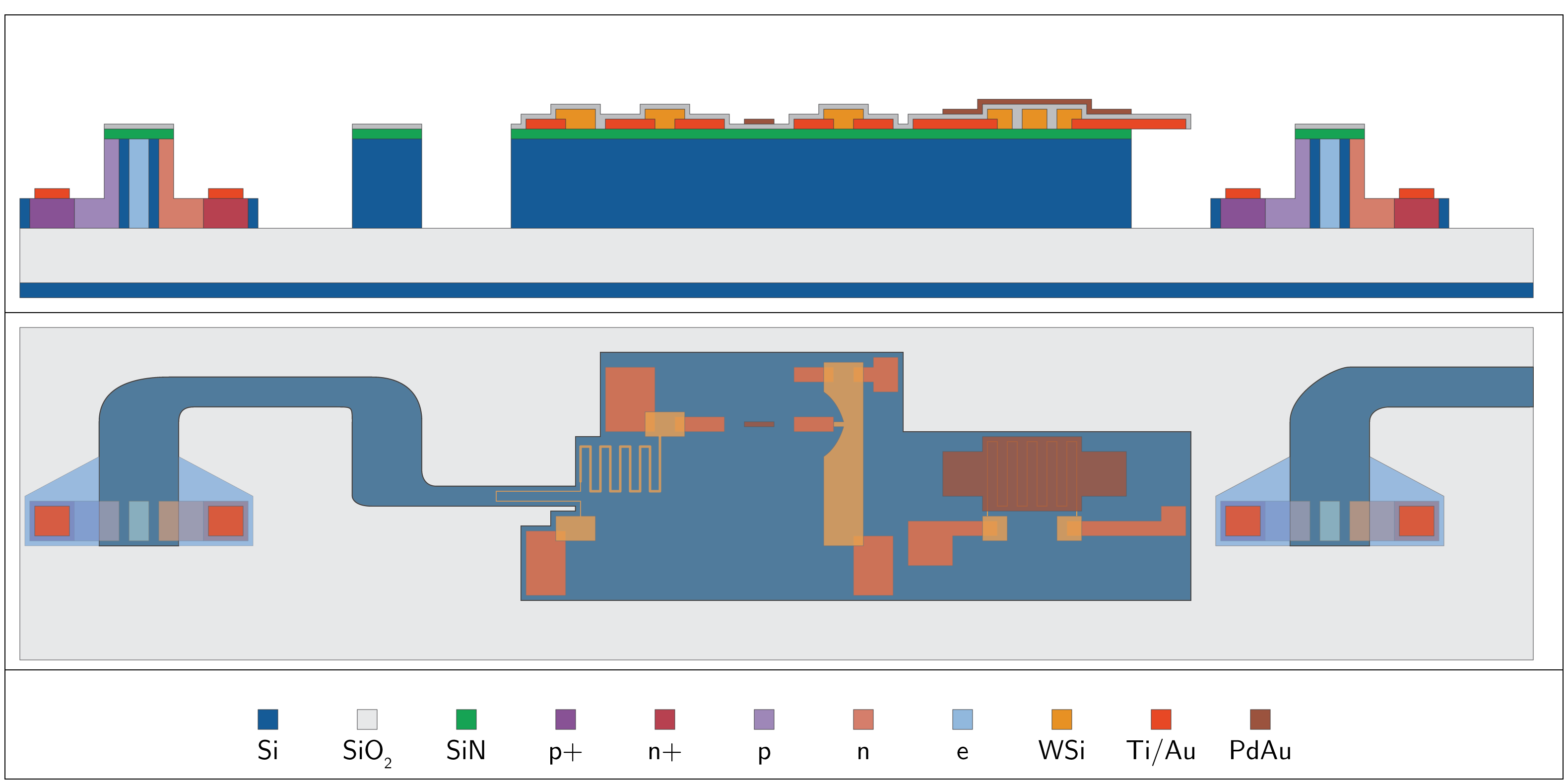
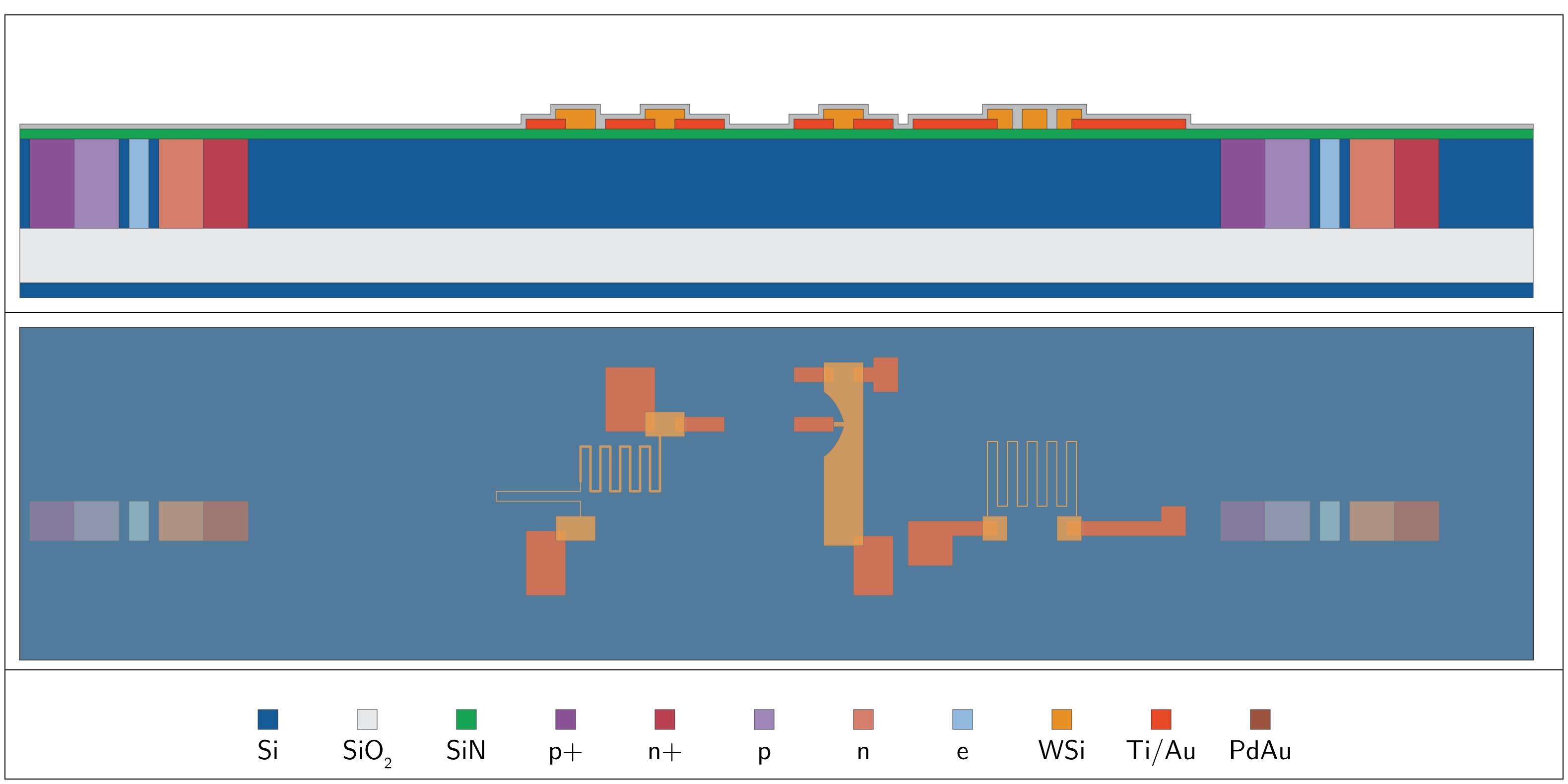
Deposit sidewall insulator

../../_images/olmc_flowImages_12-sidewallInsulator.png

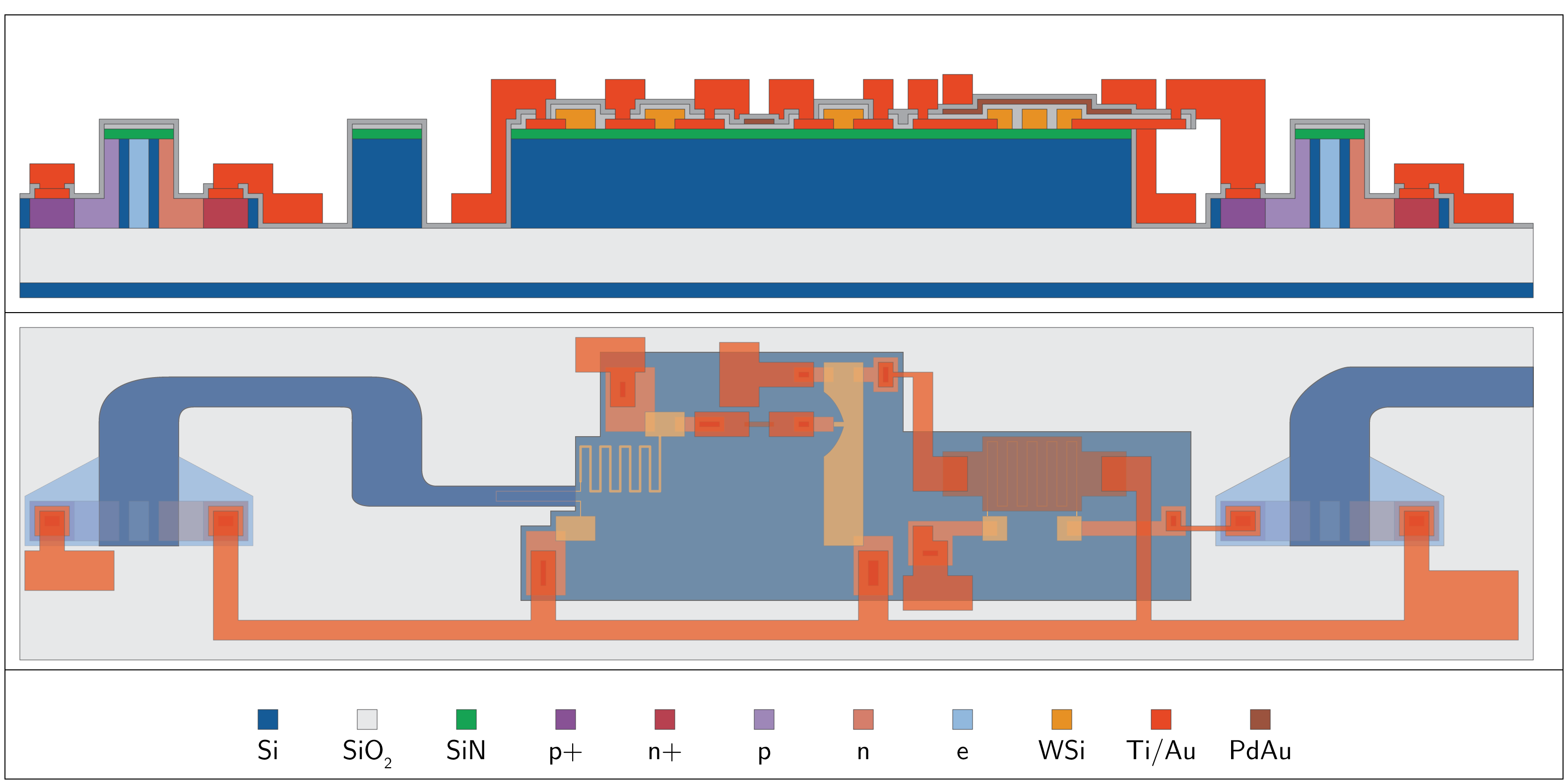
Etch vias to superconductor and LED pads

../../_images/olmc_flowImages_13-via.png

Deposit TiAu wiring layer

../../_images/olmc_flowImages_14-metal.png

Deposit top cladding

../../_images/olmc_flowImages_15-cladding.png

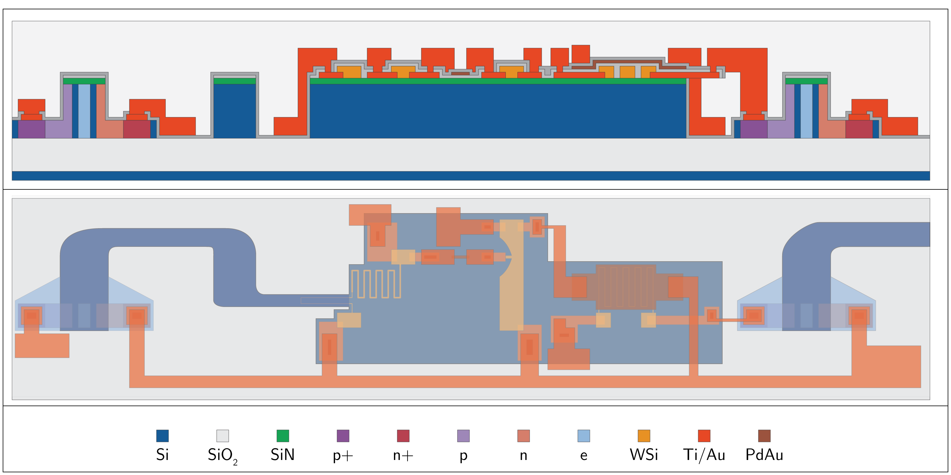
Etch vias to wirebond pads

../../_images/olmc_flowImages_16-padOpen.png