About the CHIPS Accurate Cure Kinetics, Stress, Mechanical Properties and Warpage (AWACKSM) project
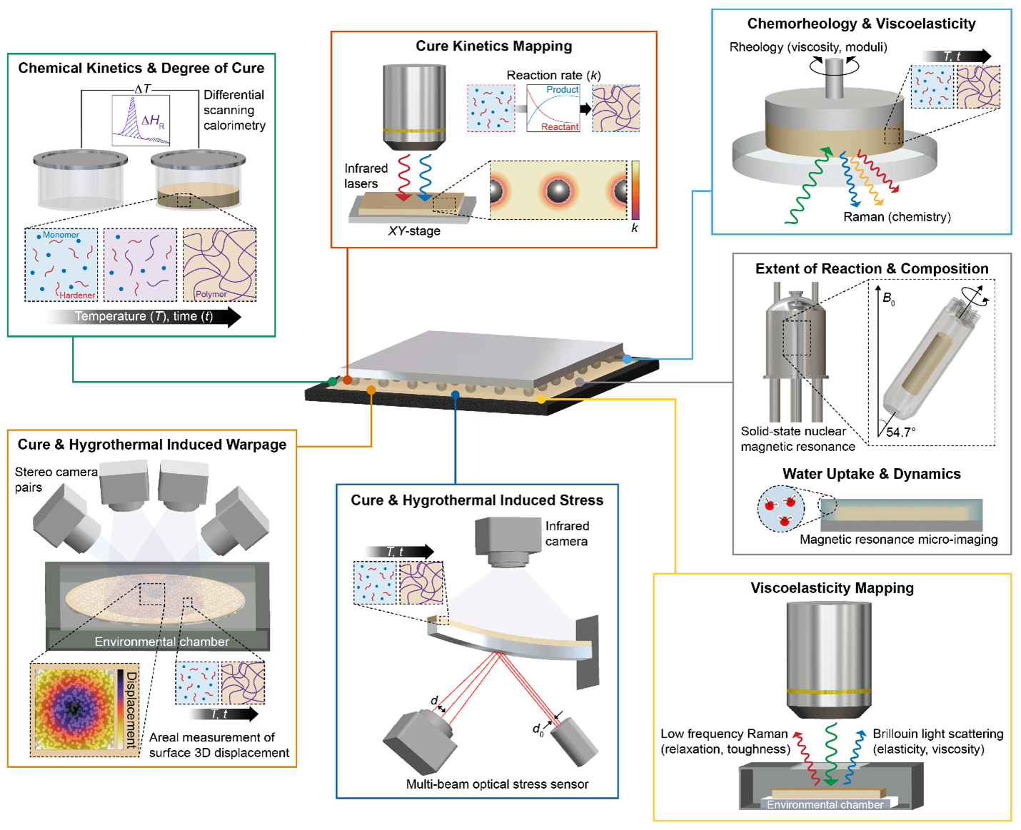
This website provides an access point to the project’s published datasets with direct links to the related files and papers. It aims to provide researchers a means to quickly understand the scope of the work and explore data relevant to semiconductor packaging materials and processing. Data is generated from the seven material measurement systems outlined in this schematic.
Click on the Data Discovery tab to browse project datasets using three filters: instrument, material, and property/measurand. You can select one or many options in each filter to narrow results. Matching files are listed below as direct links to the NIST Public Data Repository, where you can open the file record or download the source data (for example, via "save link as...").
Explore other data products from the CHIPS R&D Metrology Grand Challenges projects in the METIS Collection.
Summary
The heterogenous integration of next generation semiconductor components into devices with complicated 2D and 3D architectures increases demands on the packaging materials. These packaging materials are typically rigid polymeric resins that start out as a liquid or semi-soft solid precursor which readily flows under or encapsulate the integrated device. During assembly, the materials undergo a curing reaction where the precursors cross-link to form a rigid packaging resin. Controlling the process by which these resins transform from a liquid to a solid, including the chemical kinetics and rheological transitions, has a significant impact on the final properties of the packaging material and the ultimate performance and durability of the device.
As part of the CHIPS R&D Metrology Program Grand Challenge 3, the focus of this project is to develop accurate cure kinetics, stress, mechanical properties, and warpage measurements to quantify the critical properties of the polymeric packaging resins of next-generation microelectronics package materials under device relevant conditions. The development and refinement of these measurement platforms will help equip industry and academia with both the measurement tools and data needed to develop the next generation of high-performance packaging materials.
The outputs of this project include quantitative measurement methods, open-source model materials systems, and shared materials property databases to inform the engineering design of advanced packaging systems in practice. These are being socialized with the semiconductor industry to drive polymer materials design and package design improvements required for 3D heterogeneous integration and to maintain standards modernity.
Background
The chiplet revolution is blurring the classic delineation between front-end transistor technologies and back-end assembly processes in the semiconductor industry. Whereas performance gains have been traditionally carried on the back of transistor scaling, the drive towards heterogenous integration places increasing demand on semiconductor packaging materials.
Polymers are widely used in packaging applications due to their ease of processing and compatibility. These include underfills, molding compounds, adhesives, interface materials, substrates and build-up layers. However, packaging materials of the future need to be optimized for an increasing list of demands that includes increased mechanical stability, reduced coefficient of thermal expansion match, minimized cure shrinkage, controlled residual stress generation, reduced warpage/package distortion, and low dielectric constants and dissipation in the high frequency dielectric regime. These properties all must be controlled under the harsh environmental conditions that include large temperature swings, fluctuations in relative humidity, and repeated cycles of mechanical, thermal, and electrical loading. It is becoming increasingly critical to the overall device performance to optimize the properties of the packaging materials to ensure they perform consistently and reliably under this difficult and complex array of conditions.
Epoxy Packaging Materials
The semiconductor industry has in general relied on a handful base polymer chemistries (e.g., epoxies, cyanate esters, acrylates) for their packaging resins for decades, and the commercial formulations have evolved to contain a myriad of proprietary reactive diluents and inert fillers that are added to the base resins to optimize the final properties. Commercial formulations are also often proprietary blends of different base polymer chemistries, a situation that leads to multiple and complicated reaction pathways.
Mission
As we now ask these materials to perform under more extreme conditions, the lack of detailed information about basic resin chemistry and composition becomes a technical roadblock to improving packaging design. It is difficult to predict how these materials will respond to the harsh conditions and high-performance environments to which they are exposed and establish quantitative structure-processing-property relationships that connect materials chemistry to performance.
Project Aims and Scope
Our project team at NIST is developing a two-pronged approach to close this gap and assist the packaging community in developing their next generation of packaging technologies. First, the team will introduce a series of model packaging material systems that will serve as test vehicles to push the development of next-generation packaging materials and measurements. These model materials will be open platforms where all aspects of the chemical composition of the system and materials properties critical for packaging will be characterized, documented, and publicly shared. Second, the team will develop a metrology suite to fully characterize the properties and performance of these model materials under device packaging relevant conditions. These measurements include quantifying the chemical kinetics of the cross-linking reactions, the degree of cure of the system, the chemo-rheology as the system converts from a liquid or semi-solid into a rigid cross-linked network, the cure-induced shrinkage of the material, mapping of the local mechanical and viscoelastic properties of the resin at the micro-scale, and the resulting cure-induced stresses and warpage. In parallel, we are developing metrology to quantify the coefficient of thermal expansion, moisture uptake as a function of relative humidity, and mechanical properties of the materials under environmentally relevant conditions.
These properties will then be correlated with quantitative warpage and distortion measurements, also under development, to develop a comprehensive understanding of how the chemistry, processing and properties of the packaging materials affect performance. Our objective is to have this platform enable molecular design cues on how to improve packaging material formulations, optimize processing strategies, serve as benchmarks for comparing different commercial formulations, and generate databases of the fundamental materials properties to facilitate the design of next generation packaging strategies.
Data Discovery Interface
Use this page to discover dataset files by combining filter selections for instrument, material, and property/measurand. The filter panel supports multi-select in each category so you can quickly compare related measurement methods, materials systems, and reported properties. Results update automatically and are grouped by dataset; each file name is a clickable link to its record in the NIST Public Data Repository for viewing metadata and downloading data files. When the glossary is open, any instrument, material, or property you select in the filters is highlighted.
Datasets
-
A Dual Mode Brillouin/Low-Frequency Raman Spectroscopy Microscope for Local Mechanical Property Imaging for Semiconductor Packaging Materials
Authors: Sebastian Engmann, Andrew J. Gayle, Stian K. Romberg, Christopher L. Soles, Chris A. Michaels
First released: 2025-05-15 (revised 2026-04-27)
https://doi.org/10.18434/mds2-3725 — Data Dictionary (CSV)
Keywords: Brillouin light scattering spectroscopy, Low-frequency Raman spectroscopy, Microscopy, In situ, Kinetics.
-
Advanced Metrology Suite for Linking Residual Stress to Fundamental Properties of Thermoset Packaging Materials
Authors: Polette Centellas, Stian Romberg, Gery Stafford, Karl F. Schock Jr., Huong Giang Nguyen, Ran Tao, Alexander K. Landauer
First released: 2025-02-06
https://doi.org/10.18434/mds2-3698 — Data Dictionary (CSV)
Keywords: Encapsulant cure kinetics, Cure shrinkage, Residual stress, Digital image correlation.
-
Advanced Characterization of the Cure Kinetics of a Liquid Encapsulant
Authors: Ran Tao, Anthony P. Kotula, Jianwei Tu, Young Jong Lee
First released: 2025-05-15
https://doi.org/10.18434/mds2-3702 — Data Dictionary (CSV)
Keywords: Microelectronics, Encapsulation, Optoelectronics, Cure kinetics, Rheology, Advanced packaging.
-
A Switchable Longitudinal & Shear BLS Microscope for Comprehensive Modulus Imaging of Semiconductor Packaging Materials
Authors: Andrew J. Gayle, Sebastian Engmann, Ran Tao, Andrew G. Korovich, Polette Centellas, Yvonne B. Gerbig, Christopher L. Soles, Chris A. Michaels
First released: 2026-05-21
https://doi.org/10.18434/mds2-4059 — Data Dictionary (CSV)
Keywords: Brillouin light scattering spectroscopy, Microscopy, Mechanical properties, Packaging, Polymers.
-
Controlling the Reaction Pathway to Tune Packaging Epoxy Properties
Authors: Polette Centellas, Ran Tao, Huong Giang Nguyen, Jan Obrzut, Andrew Korovich, Alexander Landauer
First released: 2026-05-21
https://doi.org/10.18434/mds2-4101 — Data Dictionary (CSV)
Keywords: Epoxy, Thermoset, Thermal curing, Moisture properties, Coefficient of thermal expansion, Residual stress.
File Count Visualization of Discovered Files
These charts summarize the meta-information on instrument, material, property/measurand, and file type by counts, plus the distribution of files per dataset. They reflect the files found under the settings specified in the Data Discovery tab. Since this is a meta-analysis, the visualizations only show the counts of files rather than underlying measurement data. Use the Measurement Data Visualization tab (under construction) for display of the dataset contents.